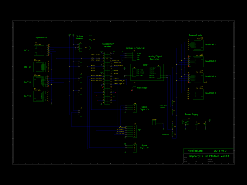
Hive Interface Board Designs
The schematics were captured and Printed Circuit Board (PCB) layout was done using GPL Electronic Design Automation gEDA tools. Most major distributions have packages that are easy to install. Version 0.3 is the current production model. In addition to the sch and pcb files, you will need the custom symbols (for gEDA schematic) and footprints (for gEDA PCB).
All the CAD tools and files are included on the HiveTool images. To access them from the Pi
From the start menu, go to
Electronics-> gEDA Schematic Editor
or
Electronics->PCB Designer.
The cad files for the 0.3 board are:
/home/hardware/hiveHAT3/hiveHAT31.sch
/home/hardware/hiveHAT3/hiveHAT34.pcb
Contents
Version 0.1
Obsolete do not use Schematics and PCB layout files (Zipped file 158K)
Why is this so big? Or why are the others so small?
Version 0.2
Obsolete do not use Schematics and PCB layout files (Zipped file 20K)
Version 0.3
Superseded by version 1.0 do not use
For details see Hardware: Hive Interface Board 0.3
Schematics and PCB layout files (Zipped file 33K)
Version 0.4
R&D Alpha with known problems. Do not use. Schematics and PCB layout files (Zipped file 689K)
Version 0.5
Current R&D model. For details, see Hardware: Hive Interface Board 5
Version 1.0
Current production model. For details see Hardware: Hive Interface Board 1.0
Symbols
Custom symbols for gEDA Schematic (Zipped file 8K)
Footprints
Custom symbols for gEDA Schematic (Zipped file 76K)
