Difference between revisions of "Change: Interface PCB"
(→Background) |
|||
| Line 31: | Line 31: | ||
*Board B will have all the connectors installed in a bulkhead configuration. It will connect to Board A by directly plugging into a header on Board A or connect via a ribbon cable. | *Board B will have all the connectors installed in a bulkhead configuration. It will connect to Board A by directly plugging into a header on Board A or connect via a ribbon cable. | ||
| + | |||
| + | ==Design Requirements== | ||
| + | Must have reliable serial communication to the Pi. Probably should use SPI bus. | ||
Revision as of 03:16, 24 January 2016
Background
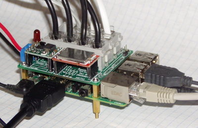
A Printed Circuit Board (PCB) has been designed and manufactured. This is an interim solution - a step towards the goal of a complete turnkey system.
- All sensor plug in.
- 12 VDC power supply with battery voltage monitoring
The goals were to
- make it quicker and easier to build a system and to make it more reliable.
- to establish a relationship with a board house.
- to select an open source pcb layout package and learn how to use it.
- to test the footprint of the RJ connectors and mating with the Pi.
Problems
- ADC is only one channel.
- No Real Time Clock (RTC).
- Board does not meet Pi HAT specification.
- Board is not general purpose but limited to our use.
Proposed change
Split this board in two, Board A and Board B.
- Board A will be a general purpose interface board that meets the Pi HAT specifications and contains:
- at least one 4 channel ADC so each load cell will be individually measured instead of being summed.
- Real Time Clock with battery backup.
- Configuration ROM
- Power supply
- Board B will have all the connectors installed in a bulkhead configuration. It will connect to Board A by directly plugging into a header on Board A or connect via a ribbon cable.
Design Requirements
Must have reliable serial communication to the Pi. Probably should use SPI bus.
