Difference between revisions of "Change: Interface PCB"
(Created page with "These are to tide us over until we get our board designed.") |
(→Design Considerations) |
||
| (14 intermediate revisions by the same user not shown) | |||
| Line 1: | Line 1: | ||
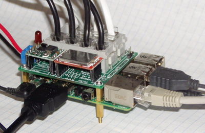
| − | + | [[File:P1010016c.jpg|thumb|400px|Dev Kit PCB installed on a Pi 2.]] | |
| + | ==Background== | ||
| + | A Printed Circuit Board (PCB) has been designed and manufactured. This is an interim solution - a step towards the goal of a complete turnkey system. | ||
| + | |||
| + | *All sensor plug in. | ||
| + | *12 VDC power supply with battery voltage monitoring | ||
| + | |||
| + | The goals were to | ||
| + | |||
| + | #make it quicker and easier to build a system and to make it more reliable. | ||
| + | #to establish a relationship with a board house. | ||
| + | #to select an open source pcb layout package and learn how to use it. | ||
| + | #to test the footprint of the RJ connectors and mating with the Pi. | ||
| + | |||
| + | ==Problems== | ||
| + | |||
| + | #ADC is only one channel. | ||
| + | #No Real Time Clock (RTC). | ||
| + | #Board does not meet Pi HAT specification. | ||
| + | #Board is not general purpose but limited to our use. | ||
| + | |||
| + | ==Proposed change== | ||
| + | |||
| + | Split this board in two, Board A and Board B. | ||
| + | |||
| + | *Board A will be a general purpose interface board that meets the Pi HAT specifications and contains: | ||
| + | #at least one 4 channel ADC so each load cell will be individually measured instead of being summed. | ||
| + | #Real Time Clock with battery backup. | ||
| + | #Configuration ROM | ||
| + | #Power supply | ||
| + | |||
| + | *Board B will have all the connectors installed in a bulkhead configuration. It will connect to Board A by directly plugging into a header on Board A or connect via a ribbon cable. | ||
| + | |||
| + | ==Design Considerations== | ||
| + | #Minimum of 8 (4 differential) inputs. | ||
| + | #Must have reliable serial communication to the Pi. Probably should use SPI, I2C bus. | ||
| + | #Consider using 16 bit ADC instead of 24 bit. | ||
| + | #Conversion speed (samples per second). | ||
| + | #Will gain of 64 work? Currently using x128. | ||
| + | #Extra ADC channels. | ||
| + | #Extra GPIO pins. | ||
| + | #Channels individually configurable. | ||
Latest revision as of 23:29, 3 March 2016
Background
A Printed Circuit Board (PCB) has been designed and manufactured. This is an interim solution - a step towards the goal of a complete turnkey system.
- All sensor plug in.
- 12 VDC power supply with battery voltage monitoring
The goals were to
- make it quicker and easier to build a system and to make it more reliable.
- to establish a relationship with a board house.
- to select an open source pcb layout package and learn how to use it.
- to test the footprint of the RJ connectors and mating with the Pi.
Problems
- ADC is only one channel.
- No Real Time Clock (RTC).
- Board does not meet Pi HAT specification.
- Board is not general purpose but limited to our use.
Proposed change
Split this board in two, Board A and Board B.
- Board A will be a general purpose interface board that meets the Pi HAT specifications and contains:
- at least one 4 channel ADC so each load cell will be individually measured instead of being summed.
- Real Time Clock with battery backup.
- Configuration ROM
- Power supply
- Board B will have all the connectors installed in a bulkhead configuration. It will connect to Board A by directly plugging into a header on Board A or connect via a ribbon cable.
Design Considerations
- Minimum of 8 (4 differential) inputs.
- Must have reliable serial communication to the Pi. Probably should use SPI, I2C bus.
- Consider using 16 bit ADC instead of 24 bit.
- Conversion speed (samples per second).
- Will gain of 64 work? Currently using x128.
- Extra ADC channels.
- Extra GPIO pins.
- Channels individually configurable.
